INTRO

Your Partner in Advanced Micro-Patterning

Step into the future of technology with K-FAB's cutting-edge printing systems designed to break barriers and transform industries.

"Our mission at K-FAB is to foster global collaboration by making semiconductor fabrication facilities accessible to researchers everywhere."

- K-Fab Team
alternative
>

Our Vision in Action

At K-FAB, we have revolutionized semiconductor fabrication by eliminating the traditional constraints of high vacuum and temperature processes, enabling submicron patterning in research. Our technology has paved the way for breakthroughs in diverse fields, from agricultural sensors that enhance crop yield and sustainability, to life-saving medical devices that improve patient outcomes, and advanced automotive components that elevate safety and performance. These achievements highlight the transformative power of accessible, collaborative technology in driving innovation and delivering real-world benefits to society.


Our Achievements

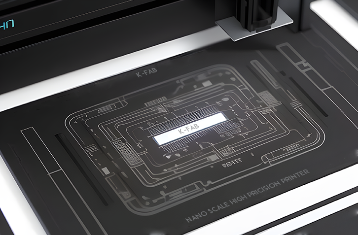
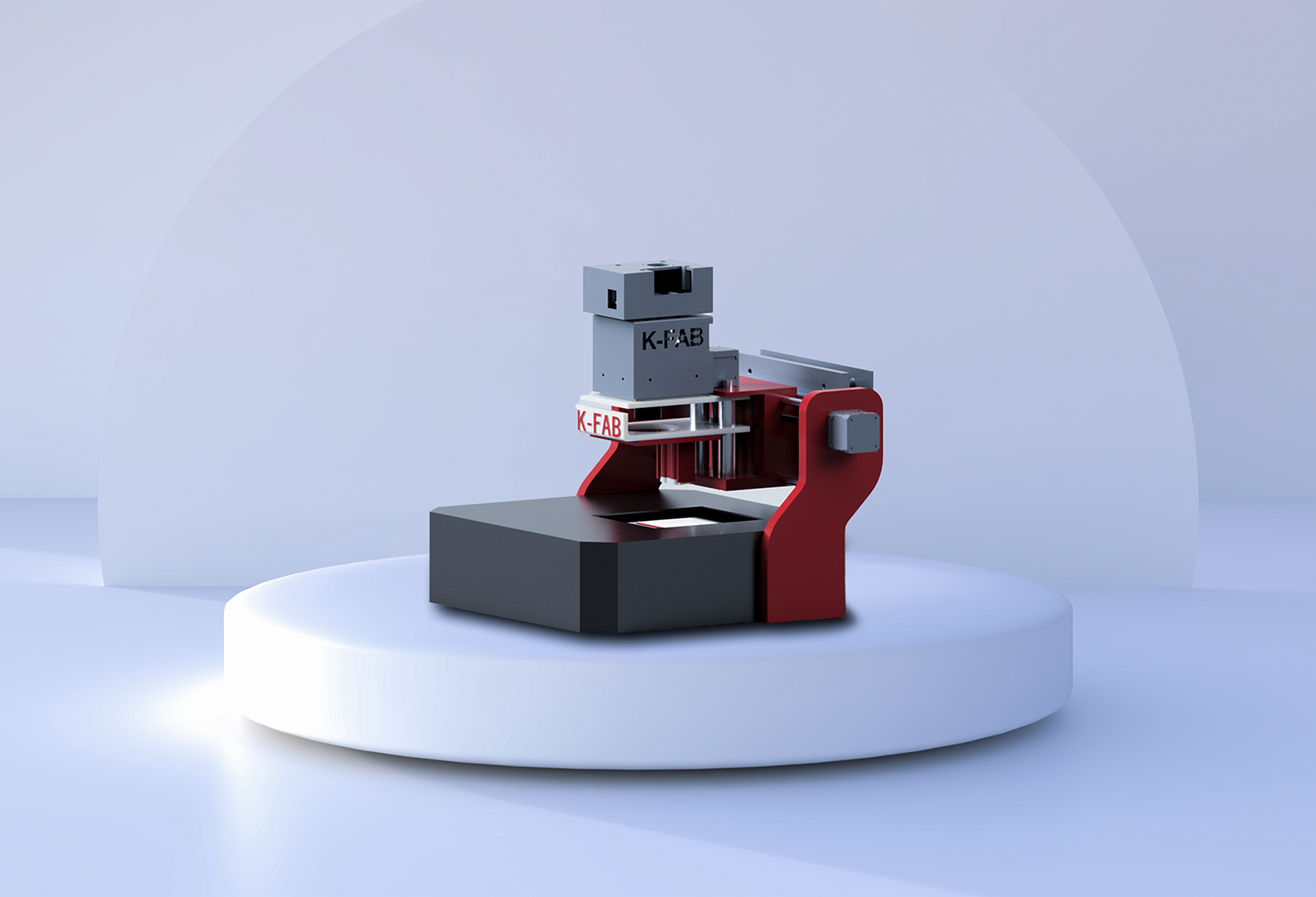
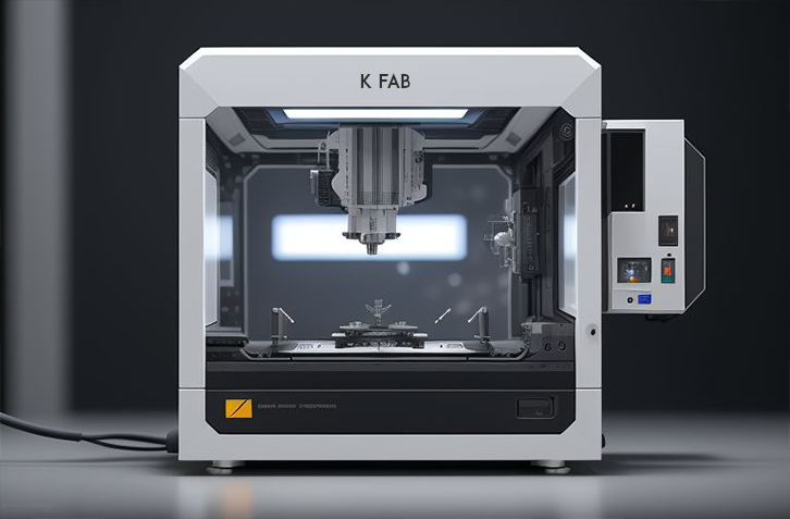
We have democratized semiconductor fabrication by providing cutting-edge, affordable facilities that empower both researchers and industries. Our innovative low-cost system enables submicron patterning without traditional high vacuum and temperature processes, setting new industry standards. Paired with advanced patterning and electrical characterization technology, it drives precision and efficiency. We also offer customizable modular cleanrooms tailored to specific research needs. Our collaborative community of researchers, engineers, and scientists fuels innovation in agriculture, medicine, and automotive sectors. By prioritizing sustainability and efficiency, we are advancing technology while fostering a more sustainable future.


Our Product

Our products support diverse industry applications. We offer a low-cost semiconductor fabrication system for precise submicron patterns without high vacuum and temperature processes, integrated with electrical characterization. Our facilities feature state-of-the-art patterning, high-precision instruments, and sensing chambers. We provide customizable cleanrooms for contaminant-free research, along with training, collaborative projects, and technical support. Our products enhance precision farming, medical device development, and automotive safety and performance.

PRODUCTS

Our Products

Nano Scale High Precision Printer

Explore the revolutionary K-FAB Printing System


CALL US

Have Us Contact You By Filling And Submitting The Form

You are just a few steps away from a personalized offer. Just fill in the form and send it to us and we'll get right back with a call to help you decide what service package works.

  • It's very easy just fill in the form so we can call
  • During the call we'll require some info about the company
  • Don't hesitate to email us for any questions or inquiries
I agree with K-FAB's stated Privacy Policy and Terms & Conditions

Founder's Of K-FAB

We're only as strong and as knowledgeable as our team.

alternative
ABOUT

We're Passionate About Delivering Growth Services

Early adopters to use our printing system.

  • Centre for Materials for Electronics Technology
  • Indian Institute Of Technology Guwahati
CONTACT

Get In Touch Using The Form

Join us at K-FAB Tech, where innovation knows no bounds, and together, let's shape the future of semiconductor fabrication.

Follow K-FAB On LinkedIn

I agree with K-FAB's stated Privacy Policy and Terms Conditions